
A Comparison of Conductive Coatings for EMI Shielding Applications, Part I
Introduction
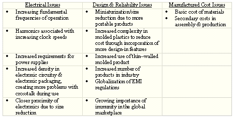
The increasing importance of conductive coatings for EMI shielding has resulted from the greater use of plastic materials in product design. Because plastics are nonconductors and are transparent to electromagnetic waves, the incorporation of a conductive coating has become an important method of providing EMI shielding to digital electronic products manufactured using plastic enclosures. Choices of conductive coating materials are based on electrical, design and reliability issues and manufacturing cost issues (Table 1).
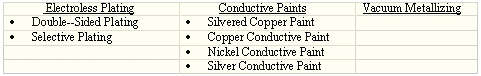
The principle types of conductive coatings used to achieve EMI shielding include electroless plating, conductive paints and vacuum metallization. Within each of these three types of coatings, there are several variations (Table 2).
Electroless Plating
Electroless shielding is based on an autocatalytic, chemical plating process, which produces a pure, continuous and uniform coating of metal to achieve EMI shielding of electronic enclosures. These coatings are duplex coatings consisting of a layer of electrolessly deposited pure copper with an overcoat of electrolessly deposited nickel–phosphorous alloy (4 to 10%P). Each layer provides specific performance benefits and contributes in a synergistic manner to the overall effectiveness of the shield. The thin, highly conductive layer of copper provides excellent conductivity for E-field and plane wave shielding effectiveness. The primary function of the electroless nickel–phosphorous topcoat is to protect the copper sub–layer from oxidation and corrosion. Additionally, the nickel topcoat provides abrasion and wear resistance due to its high as–plated hardness. Furthermore, the electroless nickel coating functions as an excellent paint base when required in post–finishing operations.
Electroless shielding processes can be applied over the entire part to achieve complete metallization of an enclosure or selectively, to metallize only specified areas. Selective plating proceeds in the same manner as the conventional double–sided process after masking of selected parts, but plating only takes place on those areas where the basecoat has been applied.
The shielding effectiveness and inherent conductivity of the part, whether it is processed selectively or by conventional means, are primarily functions of the thickness of the copper. Surface resistivity or impedance is also influenced by the smoothness of the surface for a given copper thickness. For most applications, the copper and nickel thicknesses necessary to meet normal FCC performance requirements are in the ranges given in Table 3.
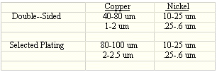
In the case of electroless nickel, a thickness of 10 to 25 gin is normally sufficient to provide the underlying copper film and also to provide adequate durability. Increased thicknesses of electroless nickel can be achieved readily through longer immersion times. In some cases, greater thicknesses of nickel are desired to accommodate certain attachment procedures, such as soldering, or to further improve corrosion and wear performance. Nickel thicknesses of 200 to 500 on (5 to 12.5 gm), for example, can be achieved when needed. Other metals, such as tin, can also be plated onto the nickel if desired.
Seleco, Inc., 8427 Zionsville Road, PO Box 68809, Indianapolis, IN 46268 Phone: (317) 872-4148 Fax: (317) 875-3276.
By Edwin Bastenbeck, Brian Jackson, Peter Kuzyk and Gary Shawhan of Enthone-OMI
Next week, we will explore Conductive Paints.